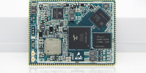
Overview
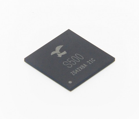
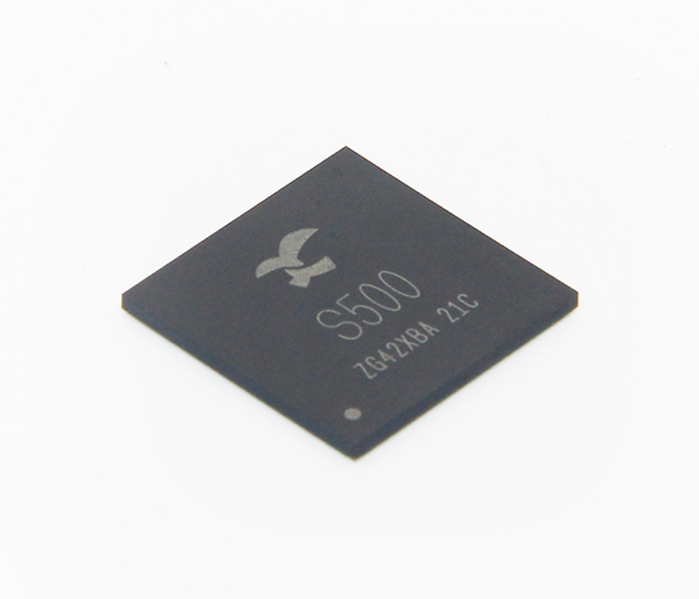
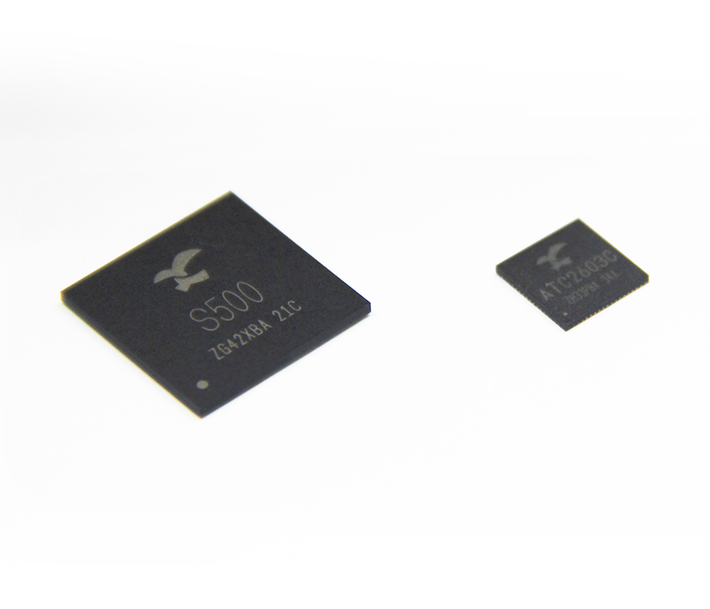
S500 SoC (System on Chip) is a high performance application processor. It integrates Quad-Core Cortex-A9R4 processor with NEON (advanced SIMD) co-processor and VFPv3 instructions set. PowerVR SGX544 GPU provides the best game experience and Full HD displays. Independent VPU (Video Processing Unit) supports almost full video formats.
S500 provide rich interfaces such as HDMI, USB, SDIO, etc. Bluetooth, WiFi and Displays peripherals are easy and fast to integrate to construct flexible solutions. High performance DDR3/DDR3L/LPDDR2/ LPDDR3 controller and large capacity NAND Flash Controller with 72-bit ECC/Toggle NAND allow engineers to build effective memory system.
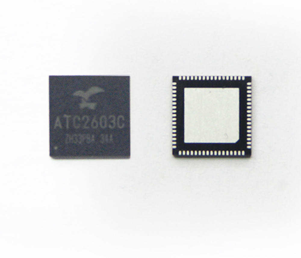
Together with Actions’ in-house designed companion chip ATC260x which integrated PMU (Power Management Unit) and Audio Codecs together, S500 really makes it the best choice for high performance products with reasonable price.
Features
Leopard II CPU
● ARM Cortex-A9 R4 CPU
● Low power and efficient multi-core architecture provides effective single-core, dual-core, and quad-core applications
● Fully comply to ARM cortex V7A instruction set 32KB L1 instruction cache, 32KB L1 data cache with 4-way set associative integrated
● 512KB L2 Cache, with 16-Way set associative L2 Cache
● Harvard level 1 memory system with MMU (Memory Management Unit)SCU (Snoop Control Unit) interface in charge of memory coherency between the four CPUs
● GIC (General Interrupt Controller) supported
● NEON (advanced SIMD) and VFPv3 D-32 instructions supported, accelerating the performance of multimedia applications such as 3D graphics and image processing
● Supporting VFP (Vector Floating Point) architecture and compliant with the IEEE 754 standard for floating-point calculation
● In-order pipeline with dynamic branch prediction equipped
● Full Coresight debug solution
● ARM TrustZone supported
GPU
● PowerVR SGX544MP
● Industry standard API support – OpenGL-ES 1.1 and 2.0, OpenVG 1.0.1
● Texture support
– Cube Map
– Projected Textures
– Non square Textures
– Volume Textures
– Texture Arrays
● Texture Formats
– RGBA 8888, 565, 1555, 1565
– Mono chromatic 8, 16, 16f, 32f, 32int
– Dual channel, 8:8, 16:16, 16f:16f
– Compressed Textures PVR-TC1, PVR-TC2, ETC1
– Programmable support for all YUV formats
● Resolution Support
– Frame buffer max size = 4096*4096
– Texture max size = 4096*4096
– Max volume extent = 2048
– Max texture repeat = 8192
Video Decoder
● Support Real-time video decoder of most popular video formats (some are supported by the 3rd party applications), such as MPEG-4, H.264, etc.
● Error detection and concealment support for all video formats
● With 2D reference data cache to reduce DDR bandwidth
● Output data format is YUV420 semi-planar
● Average data rate 60Mbps, peak rate up to 120Mbps
Video Encoder
● Support video encoder for baseline H.264
● Input data formats:
– YUV420SP
– YVU420SP
– YUV420P
– ARGB
– ABGR
– ARGBA
– BGRA
– RGB565
– BGR565
● Support VBR and CBR
● Max fps is up to 60fps@1920*1088, 5M pixel and 13M pixel
● Video size from 176*144 to 1920*1088
● Support upscale and downscale, from 1/2 to 8
● Low latency data encoder
JPEG Decoder
● Input JPEG file : YCbCr 4:0:0, 4:2:0, 4:2:2, 4:4:4 ,211H, 211V sampling formats
● Output raw image : YCbCr 4:0:0, 4:2:0, 4:2:2, 4:4:0, 4:1:1 and 4:4:4 semi-planar
● JPEG Baseline Decoder size is from 48*48 to 30000*30000 (900Mpixels)
● For Progressive Decoder size is from 48*48 to 8192*8192
● Support JPEG ROI (Region of Image) decode
● Maximum data rate is up to 100 million pixels per second
JPEG Encoder
● Input data format:
– YUV420sp
– YVU420sp
– YUV420P
– ARGB
– ABGR
– ARGBA
– BGRA
– RGB565
– BGR565
● Max data rate up to 70 million pixels per second
● Image size is from 48*48 to 8176*8176
● Support upscale and downscale, from 1/2 to 8
System Components
● DMA
● There are 12 independent DMA channels in DMA controller
● Data path is supported with memory to memory, memory to peripheral, peripheral to memory
● Support link list transfer type
● Support chain transfer type between different channels
● Support constant fill mode to initial memory
● Support stride mode for frame buffer data transfer
● Support reload mode
● The RW priority of ALL channels can be setting independently
● Support byte align transfer between memory and memory
● CMU
● One oscillator with 24MHz clock input and 7 embedded PLLs
● The DDR PLL ,NAND PLL, Display PLL have optional spread-spectrum function to reduce EMS
● clock gating control for individual components
Timer
● 2 on-chip 2Hz controllers and 2 on-chip Timer controllers inside
● Support IRQ mode
● Interrupt
● On-chip ARM Generic Interrupt Controller V2.0 support
● Maximum of 5 PPI interrupts for each Cortex-A9 interface and 58 SPI interrupt sources input from different modules
● Maximum of 16 Software Generated Interrupts for each Cortex-A9 processor interface
● Support software-programmable interrupt priority for each interrupt source
● Two separated interrupt outputs (nFIQ and nIRQ) for each processor
● E-FUSE
● 256-bit E-FUSE equipped
● HDCP2 TX
● Uses industry-standard public-key RSA authentication and AES-128 encryption
● Compliant to HDCP revision 2.1 and 2.0
● Supports repeaters
● Inside Random Number Generator compliant to NIST-SP 800 90
● Inside HMAC-SHA256 block
● Inside Input and Output FIFO for raw and Encryption datum
● Inside TS packet compliant to Blue-Ray and MPEG2 format
● Supports PES portion Encryption mode
Internal Memory
● BOOT ROM
● Size : 32KB
● Support boot from the following device:
● Emmc (SD2 Controller)
● NAND Flash
● SD/TF card (SD0 Controller)
● SPI NOR Flash
● SPI NAND Flash
● USB driver is inside for firmware upgrade and hardware test
● SRAM
● Size : 72KB
External Memory
● DRAM
● DDR3 / DDR3L / LPDDR2 / LPDDR3 supported
● up to 2GB supported
● Internal ODT resistance to improve signal integrity
● Programmable input DQS signal calibration option, calibration period is also programmable
● Differential DQS signal to achieve stable data strobe
● Optional ZQ calibration command in programmable period
● Hardware options in DDR state manage to reduce DDR power in some low bandwidth application
● Built-in hardware monitor to improve system debug
● Built-in hardware bandwidth performance counter
● Support more than 4 command processing concurrently in one cycle
● Command reorder in some circumstance to improve bandwidth
● NAND Flash
● Support both Async (include LBA NAND) and Sync NAND Flash, up to 4 CEs
● SLC, MLC and TLC NAND Flash support
● Support Toggle DDR NAND V1.0 and Toggle DDR NAND V2.0
● Support Open NAND Flash Interface (ONFI) up to V3.0
● Up to 72bit hardware ECC
● Ready/Busy signal monitor by hardware automatically
● Support sync NAND Flash Interface up to 200MHz
● Support 3.3V and 1.8V VCCQ
● SD/MMC/EMMC
● 3 on-chip SD controller inside
● support
– SD/HCSD/SDXC (SRD50 mode), miniSD
– microSD
– memory card
– MMC/RSMMC/MMCPLUS card
– INAND
– MOVINAND
– eMMC
– SDIO card
● Support SD 3.0, SDIO 3.0 and MMC 4.5 protocol
● EMMC4.5 supported
● Support 1-bit, 4-bit, 8-bit, bus mode.
● Clock max rate up to 100MHz
● Support IRQ and DMA mode to transmit data
● Contain 512 BYTE SRAM*2
● Read/Write CRC Status Hardware auto checked
● Support Auto multi Block read/write mode
● Support boot mode based on MMC43 SPEC
● Hardware timeout/delay function.
● Integrated Clock Delay Chain Technique to Regulate Card Interface Timing
● Built-in pull up resistors for CMD/DAT lines.
Display Subsystem
● Display Engine:
● Four video layer
● ABGR8888, ABGR1555, ARGB8888, RGB565, YUV 4:2:0 planar format, YUV 4:2:0 semi-planar format
● Video1 Max input 1920*1080
● Video2~4 Max input 1920*1080
● 1/4 to 4 scale in horizontal
● 1/4 to 4 scale in vertical(YUV 4:2:0 planar and YUV 4:2:0 semi-planar)
● 1/2 to 2 scale in vertical(Other formats)
● Bicubic or bilinear scaling]
● Brightness, contrast, saturation adjustment
● Flip in horizontal and vertical
● 1/2 subsample in horizontal and vertical
● Two cursor Layer
● ARGB8888
● Max input 64×64
● Two blender and output path
– Max output 1920*1080
– Alpha blending
– Colorkey
– Dither from 24-bit to 18/16-bit
– Register double buffer
● Gamma correction
● HDMI
● Compatible with HDMI 1.4b, HDCP1.1 and DVI 1.0
● Supports most video formats from 480i to 1080p, such as:
– 640*480p@59.94/60Hz
– 720*480p@59.94/60Hz
– 720*576p@50Hz
– 1280*720p@59.94/60Hz
– 1280*720p@50Hz
– 720(1440)*480i@59.94/60Hz
– 720(1440)*576i@50Hz
– 1440*480p@59.94/60Hz
– 1440*576p@50Hz
– 1920*1080i@59.94/60Hz
– 1920*1080i@50Hz
– 1920*1080p@24Hz
– 1920*1080p@59.94/60Hz
– 1920*1080p@50Hz
● Supports 24-bit, 30-bit, 36-bit RGB/YCbCr 4:4:4 format (Deep Color)
● Supports xvYCC601, xvYCC709 Enhanced Colorimetry format
● Supports IEC60958 audio format up to 24 bits
● Supports high bit rate compressed audio formats
● Supports up to 8-channel Audio sample, supports 48/96/192/44.2/88.4/176.8kHz audio sample rate
● Supports Auto-Lipsync Correction feature
● Supports 3D Frame Packing Structure up to 1080p@60Hz
● Supports 3D Side-by-Side (Half) Structure with 1080i@59.94/60Hz, 1080i@50Hz, etc.
● Supports 3D Top-and-Bottom Structure with 1080p@24Hz, 720p@50Hz, 720p@59.94/60Hz, etc.
● LCD Controller
● Support dual channel LVDS interface LCD
● Support 24-bit RGB interface
● Support MIPI DSI interface
● Programmable timing control for various panels
● Pixel stream input without strict timing requirements
● Resolutions up to 1920*1080
● Maximum 16777216 simultaneous display color
● Fill the empty field when output size is smaller than LCD display size
● Support VBI, HBI, AVSI, FEI (Frame end interrupt)
● MIPI DSI
● Compliant with MIPI DSI Specification version 1.01 and the D-PHY specification version 0.9
● Display Resolutions: QQVGA, QCIF, QVGA, CIF, VGA and WVGA
● Pixel Format:
– Command Mode: RGB233, RGB444, RGB565, RGB666(Loosely), and RGB888
– Video Mode: RGB565, RGB666 (Packed), RGB666(Loosely), and RGB888
● Command and Video mode support(type 1,2,3 and 4 display architecture)
● Low power and ultra low power support 75 Mbps to 1Gbps per lane
● Support 1-4 data lanes
● LVDS
● Comply with the TIA/EIA-644-A LVDS standard
● Support reference clock frequency range from 10MHz to 130MHz
● Support LVDS RGB 24/18 bits color data transfer
● Support VESA/JEIDA LVDS data format transfer
● Support LVDS single channel and double channel data transfer, Odd/Even channel Mirror/Swap
CMOS Sensor Interface
● Two CMOS sensor input channels
● Windowing function
● 8-bit data parallel with Hsync, Vsync, Pclk
● DVP/MIPI CSI interface
● YUV input sequence selection and storing format selection
● Max support 5M pixel input
● MIPI CSI
● Compliant with MIPI CSI-2 Specification version 1.0 and the D-PHY specification version 0.9
● High-Speed Mode : from 80 Mbps to 1 Gbps synchronous
● Low-Power Mode : spaced one-hot encoding for data
● Ultra low power supported
● Support Data Type : YUV422-8bit
● 1-4 Data Lanes Configurable
Highly-integrated Interfaces
● USB3
● Host and Device mode is supported
● Fully compliant with USB Specification 2.0
● Device mode Supports High Speed (480Mb/s) and Full Speed (12Mb/s)
● Host mode Supports USB High Speed, Full Speed and Low Speed
● Supports Control, Bulk, Isochronous and Interrupt Transfers
● Embedded USB high-speed Transceiver which complies with Interface UTMI+(level3)
● Up to 31 devices are supports by the Host
● Supports USB remote wake-up feature
● Host mode is compliant with XHCI architecture
● Downstream hub function is supported
● USB2*2
● Complies with On-The-Go Supplement to the USB2.0 Specification Revision 1.0a.
● Two independent USB2.0 controllers are inside
● UTMI+ level2 Transceiver Macrocell Interface
● HSIC Interface for an option
● Supports point-to-point communication with one low-speed, full-speed or high-speed device in Host mode (one series downstream HUB supported)
● Supports full-speed or high-speed in peripheral mode
● Supports 15 IN endpoints and 15 OUT endpoints besides Control endpoint0
● Supports high-speed high-bandwidth isochronous transfer and Interrupt transfer
● Supports suspend, resume and power managements function
● Support remote wakeup
● One OTG function and the other working as either Device or Host
● UART/IRC
● 7 on-chip UART controller inside
● 5:8 Data Bits and LSB first in Transmit and Received
● 1:2 Stop Bits
● Even, Odd, or No Parity
● 16 levels Transmit FIFO and 32 levels Receive FIFO
● Capable of speeds up to 3Mbps to enable connections with Bluetooth and other peripherals
● Support IRQ and DMA mode to transmit data
● Only UART23 support RTS/CTS Automatic Hardware Flow Control to reduce interrupts to host system
● Only UART0 support IRC(infrared remote control) Inputs
● Support RC6RC59012NEC(8-bit) protocol
● Need to connect an IR receiver when use
● Support IR Paddle
● The UART3 supports 1.8V/3.3V, configurable
● TWI
● 4 on-chip TWI controller inside
● Both master and slave functions support
● Support standard mode (100kbps), fast-speed mode (400kpbs), fast-plus-speed mode (1Mpbs), High-Speed mode (3.4Mbps)
● Multi-master capability
● Internal Pull-Up Resistor (1.5kOhm) optional
● 8-bit*128 TX FIFO and 8-bit*128 RX FIFO
● SPI
● 4 on-chip SPI controller inside
● Support master mode and slave mode. The speed of master mode up to 60Mbps, and slaver up to 20Mbps.
● 32-bit*32 TX FIFO and 32-bit*32 RX FIFO
● Support dual I/O write and read mode while use as master
● Support single data rate mode and double data rate (DDR mode) while use as master
● Support two wire mode, only use SCLK and MOSI signal
● Support IRQ and DMA mode to transmit data
● Support system program boot from SPI NOR-Flash
● Ethernet
● Supports 10/100 Mb/s data transfer rate
● Supports RMII/SMII interface
● Meets the IEEE 802.3 CSMA/CD standard
● Full or half duplex operation
● Flexible address filtering
● Up to 16 physical addresses
● 512-bit hash table for multicast addresses
● Scatter/gather capabilities
● Descriptor “ring” or “chain” structures
● Automatic descriptor list polling
● Clock switching supported
● Operates as internal configurable FIFOs
● Programmable transmit threshold levels
● PWM
● 6 independent PWM signal from 24Hz to 24MHz
● PWM with 1024-level duty adjustment
● PWM with high level or low level active
● Audio Interface
● I2S
– 2 channels (1 TX, 1 RX)
– Supports 2.0-channel I2S transmitter and receiver
– Supports 7.1-channel and 5.1-channel through I2S transmitter with ext.8-channel and 6-channel DAC by TDM (Time-Division Multiplexed) Mode
– Supports 4-channel through I2S receiver, by TDM Mode for 4-channel record
– Audio data up to 24bits
– Sample rate up to 192KHz
– Provides master work mode
● Key
● 4*3 Key matrix supported
● Support Parallel Out/Parallel In, Serial Out/Parallel In, Serial Out/Serial In, IO scan Mode;
● Support IRQ mode
● Supports programmable scan timing
OS (Operation System)
● Linux kernel 3.10
● Android 5.1.1
● Debian Linux distribution and others
Power
● 3.3V I/O power and 1.0V core power required
● Actions’ LPD Gen. IV(Low Power Design Generation IV) architecture integrated
● Actions’ ADP(Adaptive Dynamic Power) architecture integrated
● Multiple power domain supported
● Dynamic internal clock adjustment supported
● Multiple standby state supported
● High precision temperature sensor is inside
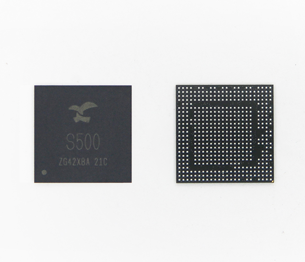
Package
● Type: TFBGA496
● Size: 16mm*16mm
● Ball pitch: 0.65mm
● Ball diameter: 0.35mm
Development Materials
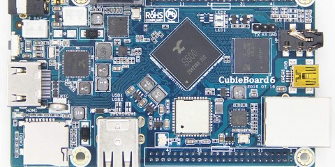
● Technical Website: http://cubieboard.org/
● Resources and Materials: http://dl.cubieboard.org/part/S500/
● DemoBoard: http://www.cubietech.com/product-detail/cubieboard6/
● Distribution contacts: sales@cubietech.com
● Technical contacts: support@cubietech.com
SOC datasheet Download link:
link: http://dl.cubieboard.org/part/S500/
SOC introduction from the Vendor:
link: http://www.actions-semi.com/en/productview.aspx?id=209